This page is an attempt to document the physical creation of an RS flip-flop (a bistable latch).
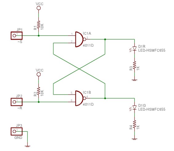
Here's the logic aspect of the schematic:
|
|
The basic logic diagram for the circuit consists of two NAND gates, the output of each connected both to an LED and an input of the other, and the unconnected input normally connected to the power supply through a pull-up resistor.
When the circuit is switched on, through logic alone which LED will turn on cannot be anticipated: if the one is zero, the other will be one (and vice versa), but at the beginning the state of neither can be determined, somewhat similar to the quantum gedanken of Schrödinger's cat. In practice, one or the other of the two states succeeds, but the concept is nevertheless fascinating to me. Also, the RS flip-flop is an example of one of the most basic (if not the most basic) implementations of memory: by connecting ground to one of the inputs of the NAND gate outputting zero, one can change its output to one and the other's to zero, and since this state reinforces itself it continues even when ground is disconnected again.
The computer software CadSoft Eagle was used for creating both the schematics and the board layout. For the schematics, everything had to be included and accounted for--not only the basic logic diagram shown. The two unused NAND gates have all their inputs connected to ground to prevent them using current unnecessarily. The two resistors connecting the power supply to two inputs are pull-up resistors, such that the voltage at the inputs will go to zero when ground is connected (all the input voltage across them, as opposed to when the entire wire from supply to input is at the same voltage). The lone ground pin is there so that it may easily be connected to one of the inputs with a wire, and the capacitor across the power supply is a decoupling capacitor, to prevent dips in the power supply when the one of the inputs is switched.
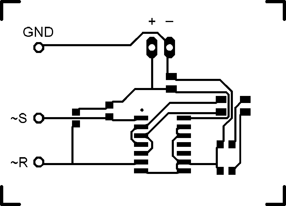
Layout:
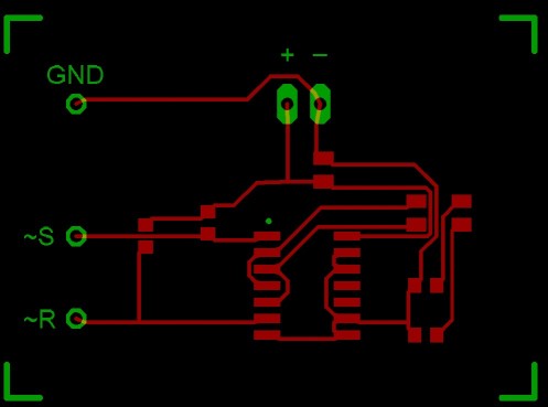
Here's the black-and-white
artwork for printing at 600dpi.
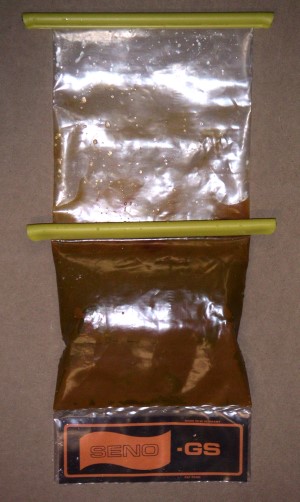
A 600 dpi ultraviolet-transparent film was printed, the layout of the circuit opaque; ultraviolet light was then shone on a photo-resist PCB through it, allowing the exposed parts to be easily removed with the application of a developer. (Note: the board was washed between the stages which involved chemicals.) Just a photoresist mask remaining over copper, the board was then etched with acid, only a fibreglass substrate visible where there wasn't a mask.
The etching bag:
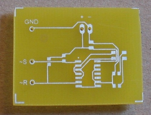
The mask was then stripped, leaving just the bare copper circuit, which was then tin-plated to make it easier to solder. Several versions of the same circuit had been made (to allow for errors), and these were separated from each other.
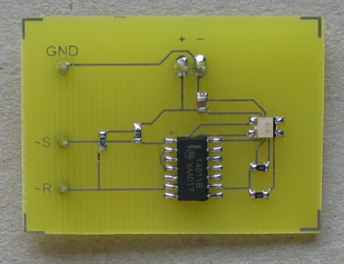
The finished board:
There were some problems with the soldering itself—one needed to hold four things in position at the same time: the small PCB, the SMT component to be soldered (some extremely small), the soldering iron, and the solder itself. To make this possible, a device was used constructed out of a coat-hanger wire attached to a thin block of wood, with one end free and firmly pressed against the block. Placing both PCB and component under the free end made it possible to use both hands to solder the two together while not having to worry about them slipping.
The device:
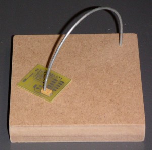
The completed project:
Once built, I'm pleased to say, the circuit worked exactly as predicted.
Parts list:
| Part | Value | Device | Package |
|---|---|---|---|
| C1 | 0.1uF | C-EU-0805 | PAS0805 |
| D1 | LED-HSMFC655 | LED-HSMFC655 | HSMFC655 |
| IC1 | 4011D | 4011D | SO14 |
| JP1 | ~S | PINHD-1X1 | 1X01 |
| JP2 | ~R | PINHD-1X1 | 1X01 |
| JP3 | GND | PINHD-1X1 | 1X01 |
| JP4 | Power | PINHD-1X2 | 1X02 |
| R1 | 10K | R-US_R0603 | R0603 |
| R2 | 10K | R-US_R0603 | R0603 |
| R3 | 1K | R-US_R0603 | R0603 |
| R4 | 1K | R-US_R0603 | R0603 |